Projects
For a full list of our publications, please visit our Publications page.
We take on a number of different projects in a wide variety of fields related to engineering. Some of the exciting projects address the issue of all-optical switching using magnetic materials. With the increasing need for fast, wide-bandwidth systems, it is advantageous to turn to optical solutions. However, in optical networks information eventually must be converted to electrical form for machine-to-machine (M2M) communication to be realized. This creates a bandwidth bottleneck in the system and limits capability. Thus, it is of interest in the research community to develop systems in which M2M communication can be realized while maintainng all-optical transfer media.
Magneto-Optic All-Optical Switches
Magneto-Optic Switching in Fiber-Optic Systems
John W. Pritchard and Mani Mina
Department of Electrical and Computer Engineering, Iowa State University, Ames, IA 50011 USA
Optical communication as a transmission media is currently the best choice for fast, long distance, and gigantic volume and bandwidth of data transfer. However, bandwidth bottlenecks are present that limit the technology, specifically at the interface where conversions between optical and electrical information take place. There are many challenges as well as new and competing technological and data analysis developments that have been proposed, considered, and implemented, which are expanding possibilities for better, faster, more bandwidth, and versatile optical communication technologies. In this article we discuss some of the wonders and some of the developments on the switching technology. The hope is to provide the reader some key concepts, issues to think and perhaps read further on, and also some references, point of technological interest, and an overview of the related technologies. In particular we will introduce magneto-optical (MO) technologies that can enable all-optical switching as valid possibilities for the current and future optical communication development. Other switching technologies are in use or have been proposed. We briefly introduce all-optical switching and then focus on MO switches and discuss them as a favorable alternative. As their current challenges are addressed, the success of MO switching technologies and the addition of knowledge to the intellectual community can be achieved. Our goal is to provide an interesting platform for general readers as well as for those interested in MO devices.
I. Introduction
Imagine, for the sake of a thought experiment, that you are sometime in the near future at your laptop computer, in the comfort of your own home. Data communication has advanced greatly and Ethernet is obsolete. Instead of plugging in those familiar copper wires to get online, you connect your optical patch cable from a spare port on your router directly to your laptop. Your speed test peaks at multiple terabits per second, and your satisfaction is achieved when your favorite series of physics video lectures is downloaded in mere seconds. This is the dream that engineers and physicists are pushing to realize. However, this dream does not end at your home.
Many applications in engineering have solutions that involve complicated systems. As technologies are refined over the years, we repeat (or copy) fundamental designs to prevent “reinventing the wheel” and make it easier to build even more complicated systems. This is common throughout many efforts in human invention, and enables fast development of technologies [1]. In such inventions involving electricity and magnetism, systems can acquire and generate information. Often times, multiple systems need to exchange this information with each other to work well. As the fundamental designs are tuned and refined, it is important that the transmission and reception of the generated or acquired information is refined as well. These tasks may not be done in parallel, which tends to create bottlenecks in the complicated systems. However, once both are refined, the entire system becomes a fundamental design, and new technologies are born.
The process of technological development is not new, but as discoveries are made the details change, and these fundamental designs may be replaced by completely different ones that are improved by orders of magnitude. This is the case with the replacement of wire-based systems by fiber-based systems. However, the replacement process is not seamless. There is currently a mix of wire- and fiber-based systems. Thus, the exchange of information between systems may require a conversion between transmission media. For fast, long-distance communication, optical communications technologies are currently the best choice. However, end-user systems convert the optical information to electronic so machine-to-machine (M2M) communication is achieved. This conversion is currently a bottleneck because electrical systems are not able to match the bandwidth capability of optical systems. Therefore, it is of great interest in the research community to reduce this bottleneck and provide an all-optical platform for communication [2]-[4].
II. Challenges in Optical Communication
Optical communications is one of the oldest forms of long distance communications technologies and is currently a rapidly advancing field. From smoke signals to light houses to visual Morse code to wavelength-division multiplexing (WDM), optical communications predates the middle ages and yet is still ever present. With the invention of silica optical fiber as the propagation medium for light and with the invention of integrated circuit technology, advanced multiplexing techniques could be utilized and higher bandwidth systems could be achieved. Furthermore, with the advancement of material purification techniques, low loss fiber (less than 0.1dB/km) was invented and optical communication became the leading low-loss, high-speed data communications technology [2]. Its current stage is the technology refinement process.
For such high speed communication platforms, encoding and decoding the signals has always been one of the main challenges. Small changes in optical signals need to be preserved and interpreted to provide the users cutting edge capabilities. In order to improve the speed the challenge is not to change the communication media and stay in the all-optical platform, however there are several ways of achieving this [4]. One of the most exciting approaches for such information encoding and decoding is via interferometric methods. Such methods mix light waves and allow for the creation and extraction of vital information. These interferometers serve as the building blocks for the advanced optical transceivers of tomorrow.
The optical-electrical-optical (OEO) interface (Figure 1) remains the major bandwidth bottleneck of optical communication networks. To reduce the effects of the OEO interface, the currently deployed electronic transceivers are to be replaced by all-optical ones [5]-[6], which can be built from combinations of interferometric modulators. Other types of all-optical systems have been proposed, but are becoming less dominant due to manufacturing efforts and long term reliability [7].

Figure 1 : Simple fiber-optic network showing OEO interfaces.
III. Interferometry and All-Optical Switches
Traditionally, interferometers are used to study the properties of materials placed in an optical path of the interferometer. Interferometers can allow one to observe how light interferes, which, in many cases, is due to changes in the state of polarization (SOP) of the light (which is usually referred to as the direction of the electric part of the optical wave) [8]. The rotation of the SOP of an incoming wave of light can be caused by reflection on (optical Kerr effect) or transmission through (optical Faraday effect) the material. Based on the resulting interference pattern, material properties can be determined. Similarly, by changing the properties of the material the interference pattern can be modified. This concept of manipulating the properties of materials to observe different interference patterns serves as the basis for all-optical switching.
Many all-optical switches of interferometer design utilize the Faraday effect. However, many different interferometer configurations can be used. Popular interferometer configurations include the Mach-Zhender, Sagnac, and resonator. Although others would suffice, these have shown to be best suited for switching applications [9]-[10].
All three configurations utilize a material that induces the Faraday effect to create a phase difference between propagating waves and cause constructive or destructive interference. The manner in which this is done make each configuration unique. The Mach-Zhender uses a coupler to split an incoming signal, rotate the SOP of one, and then combine the signals with a second coupler to create interference at the output [11]. The Sagnac uses one coupler that splits an incoming signal, each signal’s SOP is then specially rotated, the signals re-enter the same coupler and interfere at the output [11]. The resonator uses a coupler to couple light onto a ring-resonating path which builds in amplitude, is delayed with respect to the incoming signal due to the loop path travelled, and thus creates interference at the output [12]. These configurations are highlighted in their basic form in Figure 2. Of the three, it seems the resonator configuration has been most convenient due to its simplicity and stability.
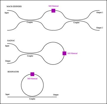
Figure 2 : Fiber-based Mach-Zehnder (top), Sagnac (center), and resonator (bottom) interferometer configurations.
Two types of the Faraday effect can be used to achieve all-optical switching. The electro-optic (EO) Faraday effect causes a rotation in the SOP of light due to an applied electric field, and the MO Faraday effect utilizes an applied magnetic field to induce Faraday rotation. Currently, EO devices dominate all-optical switching. However, with the increasing need for low-cost, low-power systems, MO devices are showing to be a sensible alternative. To realize this, a couple of the most important hurdles that need to be overcome are the inclusion of the MO Faraday rotator (MOFR) and the optimization of the magnetic field generator (MFG).
The MFG is generally a coil rapped around the MOFR, and an electronic driver circuit supplies current to create the required field. The flux density for a single coil can then be approximated to be [13]:
where ![]() is the permeability of free space,
is the permeability of free space, ![]() is the number of coil turns,
is the number of coil turns, ![]() is the current through the coil,
is the current through the coil, ![]() is the length of the coil, and
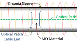
is the length of the coil, and ![]() is the coil radius. For fiber-based designs, the inclusion of the MOFR is relatively simple. A small slab of the material can be placed between the two fiber patch cables with index matching gel at the interfaces. The MFG can then be a coil wrapped around a fiber guiding sleeve. For silicon-based devices, it is not so simple. Special techniques are required to include suitable MO material such that monolithic integration is achieved. This affects fabrication capabilities. However, recent advancements in the design of integrated optical isolators have shown significant progress [14].
is the coil radius. For fiber-based designs, the inclusion of the MOFR is relatively simple. A small slab of the material can be placed between the two fiber patch cables with index matching gel at the interfaces. The MFG can then be a coil wrapped around a fiber guiding sleeve. For silicon-based devices, it is not so simple. Special techniques are required to include suitable MO material such that monolithic integration is achieved. This affects fabrication capabilities. However, recent advancements in the design of integrated optical isolators have shown significant progress [14].
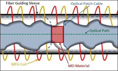
Figure 3: Cross section of inserted MO material in a fiber-based system.
The MFG for fiber-based systems is relatively simple, but is not as fast as desired. Commercial devices can achieve optical pulse widths on the order of 10 microseconds, and recent works have shown pulse widths achieved near 150 nanoseconds [15]. Yet, the complimentary practical EO devices can achieve pulse widths less than 1 nanosecond. While there are theoretical limits that may not allow us to reach 1 nanosecond, with the monolithic integration of an MO switch, the magnetic domain switching limit can be approached (within an order of magnitude compared to EO switches) and these switches can be more useful.
IV. MO Switches and What Lies Ahead
Each type of switch has different a role in the optical communications network. EO switches are advantageous in their ability to perform processing and “bit banging” operations – tasks that require very high switching speed mechanisms [16]. However, it is common in optical networks to require signal routing schemes as well. These schemes do not need very fast switching speeds, but instead require “on” and “off” times to be relatively long. In this case, MO switches that utilize hard magnetic materials can be used as a low-power solution. A hard ferrite with remanence will “latch” its magnetization direction to the direction of the applied field. This can be used to create a MO switch that can define a signal path and latch to the path for long periods of time without the continued presence of a magnetic field. If an EO switch was used in this way, the electric field would need to be present the entire time the signal path was defined, dissipating a lot of power in the process. The power-saving feature of an MO switch can directly translate to a cost-saving feature (since power requires money), but this is only advantageous if the money saved can match the cost to manufacture such a switch.
It is a continued effort to properly include MO material on silicon-based devices to realize a monolithically integrated MO switch (Figure 4). Commercial fiber-based devices with MO material have been developed, but their resulting size does not allow for large scalability. With the monolithic integration of a MOFR on silicon, the potential for fully integrated and efficient all-optical systems on a chip (SoC) can be realized. One of the main challenges in monolithically integrating a MOFR on silicon has been in matching the crystal structure of the MO material to silicon’s. In theory, this can be done by annealing the device after MO material deposition. However, the annealing temperature required for such a task results in the MO material experiencing exceedingly high optical absorption properties. In recent works, this has shown to be resolved by employing special pulsed laser deposition (PLD) techniques [14]. Once these processes have been refined and adapted to standardized CMOS processing, the MFG can be implemented. However, the consistent design and implementation of such an MFG has yet to be reported.
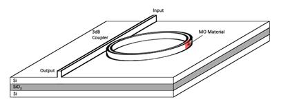
Figure 4 : Example of an integrated MO interferometric switch of resonator configuration.
On-silicon, high-amplitude MFGs oriented transverse to the silicon wafer plane have not been studied extensively. In-plane coils have been designed and implemented quite often in RF systems, however the fields generated (or received) are generally smaller than that required to achieve sufficient Faraday rotation. Thus, it is of interest to design a transverse-plane MFG that is suitable for MO switching applications. If the silicon-on-insulator (SOI) platform using rib waveguides is chosen as the optical propagation technology, then the coil would most likely be of square geometry, as shown in Figure 5. The field through such a coil may be approximated by assuming circular geometry and using (1).

Figure 5 : Example of a solenoid of rectangular geometry.
The research and development on the monolithic integration of MO technologies will open doors to new topics of interest, furthering our knowledge of the intimate relationship between light and magnetism. In addition, pursuing challenges of MFGs of such small form-factor will help us better understand domain dynamics and how to utilize them on a microscopic scale to create more interesting devices.
V. Conclusion
In this article we attempted to provide an overall perspective of some of the key issues related to high speed optical communication systems. In particular this article tried to focus on switching technologies and introduced challenges related to magneto-optical switching. Our goal was to inform the general reader about the key concepts and ideas, and provide useful references for those who would like to probe further. We hope this would ignite the reader’s interest to pursue reading, researching, and advancing the family of technologies.
VI. References
- S. J. Paley, “The Art of Invention: The Creative Process of Discovery and Design,” Amherst, NY: Prometheus, 2010.
D. K. Mynbaev, and L. L. Scheiner, “Fiber-optic Communications Technology,” Upper Saddle River, NJ: Prentice Hall, 2001.
R. Ramaswami, K. N. Sivarajan, and G. H. Sasaki, “Optical Networks: A Practical Perspective,” Amsterdam: Elsevier/Morgan Kaufmann, 2010.
J. H. Chao, and B. Liu, “High Performance Switches and Routers,” Hoboken, NJ: Wiley-Interscience, pp. 468-537, 2007.
D. Dai, J. Bauters, and J. E. Bowers, “Passive technologies for future large-scale photonic integrated circuits on silicon: polarization handling, light non-reciprocity and loss reduction,” Light: Science & Applications, 1, e1, 2012.
B. J. Sheu, and M. Ismail, “Multimedia Technology for Applications,” New York: IEEE, 1998.
X. Ma, and G.-S. Kuo, "Optical switching technology comparison: optical MEMS vs. other technologies," Communications Magazine, IEEE, vol. 41, no. 11, pp. S16- S23, 2003.
S. O. Kasap, “Optoelectronics and Photonics: Principles and Practices,” Upper Saddle River, NJ: Prentice Hall, 2001.
S. Kemmet, M. Mina, and R. J. Weber, “Fiber-Based Magneto-Optic Sagnac Optical Modulator,” Magnetics, IEEE Transactions on, vol. 45, no. 10, pp. 4892-4894, 2009.
R. Bahuguna, M. Mina, R. J. Weber, “Mach–Zehnder Interferometric Switch Utilizing Faraday Rotation,” Magnetics, IEEE Transactions on, vol. 43, no. 6, pp. 2680-2682, 2007.
P. Hariharan, “Optical Interferometry,” Amsterdam: Academic, 2003.
C. K. Madsen and J. H. Zhao, “Optical Filter Design and Analysis: A Signal Processing Approach,” New York: John Wiley, 1999. - J. A. Stratton, “Electromagnetic Theory,” New York: McGraw-Hill Book, pp. 233, 1941.
L. Bi, J. Hu, P. Jiang, D. H. Kim, G. F. Dionne, L. C. Kimerling, and C. A. Ross, “On-chip optical isolation in monolithically integrated non-reciprocal optical resonators,” Nature, vol. 5, pp. 758-762, 2012.
J. W. Pritchard, M. Mina, and R. J. Weber, “Enhanced Driver Circuit for Magneto-Optic Switching Technologies”, Magnetics, IEEE Transactions on, 2012, to be published.
L.-S. Yan, A. E. Willner, X. Wu, A.-L. Yi, A. Bogoni, Z.-Y. Chen, and H.-Y. Jiang, “All-Optical Signal Processing for Ultra-High Speed Optical Systems and Networks,” Lightwave Technology, Journal of, vol. PP, no. 99, pp. 1, 2011.
What we do
Who we are

Special Interests